

 Bulgaria


Power Management for all of Tomorrow’s Innovations
Everything needs power. Engineers are constantly seeking ways to design products that are more efficient and less power-consuming. This is where power management comes in. Analog Devices’ power management integrated circuits and power modules provide the foundation for powering new designs across all markets.
Finding the Sweet Spot for Flyback Converters in EVs
Even with advances in battery technology and electromechanics, original equipment manufacturers (OEMs) struggle to meet the mix of expectations on ultralow emissions performance, vehicle range, and consumer affordability. Innovations in isolation, power management, magnetics sensing, and battery management systems (BMS) can help OEMs meet ultralow emissions, range, and vehicle cost expectations.
Technology Innovations Will Lift the Last Hurdles to Electric Vehicle (EV) Mass Adoption
There are two significant disruptions currently affecting the future of vehicular transport and semiconductor technology. The first is shifting from the internal combustion engine (ICE) to the electric motor drive. The second is the emergence of power switches employed in motor drive systems based on wide bandgap material. These offer figures of merit in the order of ten times better than the incumbent solution based on silicon. However, with the battery accounting for more than twenty-five percent (25%) of the final vehicle cost, optimization of energy use is one of the keys to achieving mass electric vehicle (EV) adoption. Reaching this goal means recognizing that every watt (W) spent is critical, and prioritizing subsystem efficiency is a primary selection criterion in automotive system design.
Recent advancements in power management for the powertrain—including isolated gate drivers, sensing, and BMS—allow designers to be creative to improve system efficiency while keeping the system cost under control (Figure 1). This article will hone in on power management and flyback converters.

Power Management
On the road toward the highest performance, every watt matters whether the EV is in “on,” “standby,” or “sleep” mode. Cutting-edge power management solutions can further increase vehicle efficiency, which correlates to extra miles while not compromising the best electromagnetic compatibility (EMC) performance from low current/low voltage to high current/high voltage applications.
Design Challenges in High Voltage Flyback Circuits
In functionally safe systems, continuity of voltage supply is critical. Generating a local low voltage rail from the high voltage battery plays a key role. In traditional isolated high voltage flyback converters, tight regulation gets achieved using optocouplers to transfer regulation information from the secondary-side reference circuitry to the primary side. The problem is that optocouplers add significant complexity to isolated designs. Optocouplers introduce propagation delay, aging, and gain variation. All these factors complicate power supply loop compensation and can reduce reliability.
Moreover, during start-up, either a bleeder resistor or high voltage start-up circuit is required to power up the IC initially. Unless an additional high voltage MOSFET gets added to the start-up components, the bleeder resistor is a source of unwelcome power loss. Let’s look at one specific example, Analog Devices LT8316 Micropower Isolated Flyback Converter.
No Need for an Optocoupler
By sampling the isolated output voltage from the third winding, no optocoupler needs to be employed for regulation. The output voltage gets programmed with two external resistors and a third optional temperature compensation resistor. Boundary mode operation helps to achieve excellent load regulation. Because the output voltage gets sensed when the secondary current is almost zero, no external load-compensating resistors and capacitors are needed. As a result, the solution has a low component count, greatly simplifying the design of an isolated flyback converter.
Start-Up Optimization
There is no need for an external bleeder resistor or other start-up components with an internal depletion-mode MOSFET (which has a negative threshold voltage and is usually on). Once a local 12V capacitor gets charged, the depletion-mode MOSFET turns off to reduce power loss.
Ultralow Quiescent Current
Designers should implement several mechanisms to achieve ultralow quiescent current. The switching frequency should be reduced at light load while keeping the minimum current limit to reduce current while properly sampling the output voltage. In standby mode, in implementing a sixteen times (16x) reduction of its switching frequency (3.5kHz–220kHz) and keeping the preload current at less than 0.1% of total output power, the LT8316 has demonstrated a quiescent current lower than 100µA.
Extremely Wide Input Range Operation
The LT8316 is rated to operate up to 600VIN. This range can get extended by placing a Zener diode in series with the VIN pin to improve the solution scalability. The voltage drop across the Zener diode reduces the voltage applied to the chip, allowing the supply voltage to exceed 600V. With the 220V Zener diode placed in series with the VIN pin, the minimum supply voltage for the start-up is 260V, give or take, considering the voltage tolerance of the Zener diode. Note that after start-up, the LT8316 will operate normally with a supply voltage below 260V. This part achieves high peak efficiencies (Figure 2). Even with no optocoupler, load regulation at different input voltages remains tight (Figure 3).


Conclusion
Analog Devices’ products address EV design challenges by offering superior battery sensing, the highest level of automotive safety, the broadest portfolio of EV BMS devices, and the most innovative, versatile system-level solutions. Click on the link to read the full-length article detailing more about how Analog Devices is helping engineers Find the Cost and Performance Sweet Spot for Battery Management and Traction Inverter Systems Design. 
ADI LT8316 Micropower Isolated Flyback Converters
Analog Devices LT8316 Micropower Isolated No-Opto Flyback Converters sample output voltage from isolated flyback waveforms that appear on third-winding transformers.
Silent Switcher 2 for Low EMI

Many electronic products must pass electromagnetic interference (EMI) compliance tests—such as the FCC Part 15 rules in the US—before being released into the market. When a company’s product fails EMI compliance tests, the company loses control of the development process, shipping dates begin to slip, projected revenues diminish, and expenses start piling up. These tests are critical, because excessive noise can interfere with sensitive electronics within the product itself.
Electronic products must get designed from the beginning with EMI attenuation in mind. Often the EMI compliance problem lies in the product’s switching power supply. In these cases, the proper solution is prevention by using an ultralow noise switching power supply in the initial designs rather than by adding shields and filters to the product after the fact.
Silent Switcher® Architecture
To overcome these challenges, Analog Devices offers Silent Switcher® Architecture which minimizes the risk of problems caused by EMI, making µModule® Power Modules, Regulators, and Discrete DC-DC ideal for noise-sensitive applications. These power products support functions like Step-Down (Buck), Step-Up (Boost), Step-Down and Step-Up (Buck-Boost), Battery Charger, Isolated Converter, and LED driver.
Silent Switcher Technology
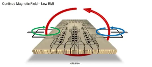
A Silent Switcher device breaks the trade-off between EMI and efficiency by not needing to slow down the switch edge rates. But how is this accomplished? Consider the LT8610 High-Voltage Buck Regulator (Figure 1). It is a 42V input-capable, monolithic (FETs inside) synchronous buck converter that can deliver up to 2.5A output current. Notice that it has a single input pin (VIN) at its top left corner.
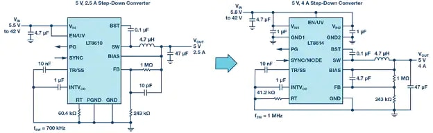
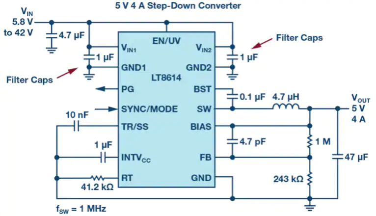
However, when contrasting the LT8610 to the LT8614 Synchronous Step-Down Silent Switcher (a 42V input-capable, monolithic synchronous buck converter that can deliver up to 4A of output current), one can see that the LT8614 has two (2) VIN pins and two (2) ground pins on the opposite side of the package. This is significant, since it is part of what makes it silent switching!
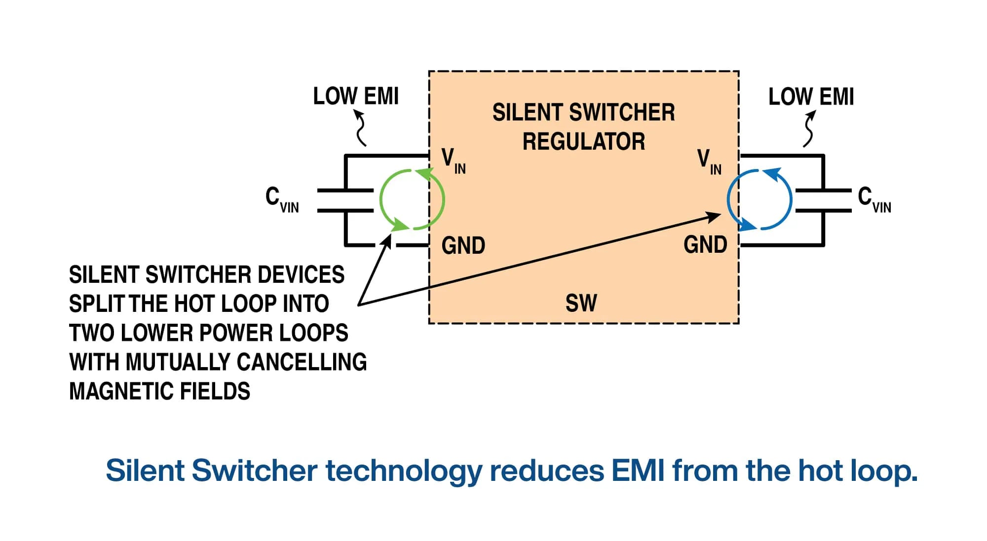
How to Make a Switcher Silent
Placing two (2) input capacitors on opposite sides of the chip between the VIN and ground pins will cancel the magnetic fields. The figure highlights this with red arrows pointing to the capacitor placement on the schematic and the demo board (Figure 2).
Highly Efficient Operation Even at High Switching Frequencies
Analog Devices Silent Switcher architecture offers high efficiency at high switching frequencies ( >2MHz) with ultralow EMI emissions, offering very compact solutions while optimizing high efficiency at light load with ultralow quiescent current (IQ). The Silent Switcher family uses a unique design and packaging techniques to offer 95% efficiency at 2MHz while effortlessly passing the Comité International Spécial des Perturbations Radioélectriques (CISPR) 25 Class 5 Peak EMI limits.
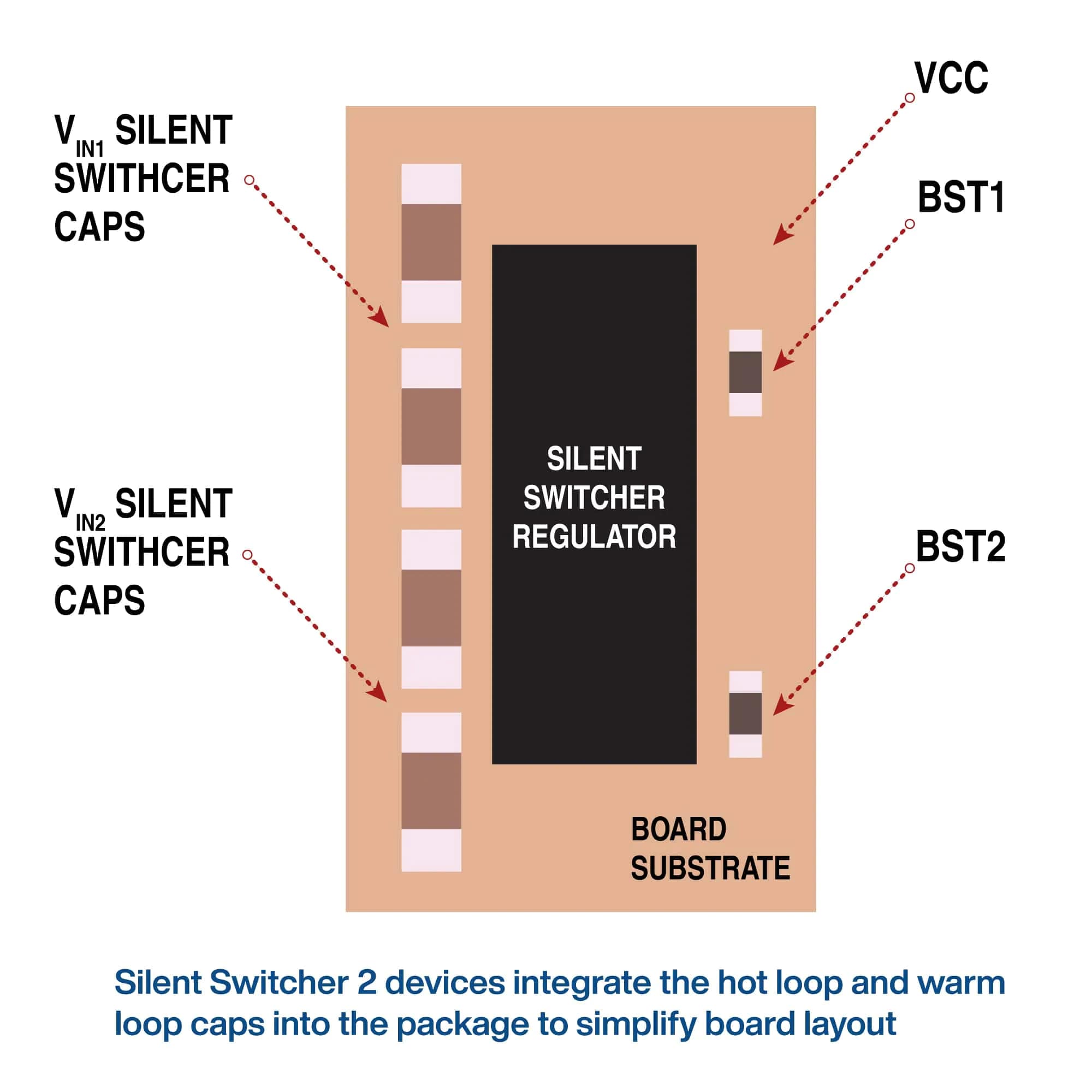
Eliminates PCB Layout Sensitivity
The Silent Switcher 2 Regulators’ design, exceptional EMI/EMC performance, and small overall solution size eliminate printed circuit board (PCB) layout sensitivity (Figure 3). The Silent Switcher 2 Regulator series features allow these devices to get employed on any PCB, simplify product design, and reduce risks even when using two‑layer PCBs ( Figure 4 ).
A synchronous buck converter produces a regulated voltage lower than its input voltage. It enables designers to deliver high currents while minimizing power loss. Analog Devices LTC3310S Synchronous Step-Down Silent Switcher® 2 DC-DC Converter achieves low EMI and high efficiency at switching frequencies as high as 5MHz. The device can provide up to 10A output current from a 2.25V to 5.5V input supply in a compact 3mm x 3mm LQFN package. It’s ideal for automotive applications, servers, telecom power supplies, and more. LTC3310S also includes a power good signal when the output is in regulation, output overvoltage protection, thermal shutdown, a temperature monitor, clock synchronization, mode selection, and output short circuit protection.
Conclusion
Silent Switcher capabilities and benefits make it easier for your switch mode power supply designs to pass the various noise immunity standards such as CISPR 32 and CISPR 25.
Current Sensing with PMBus Digital Power Systems Managers
Board-level designers are tasked with giving life to a board, monitoring its health, adjusting settings, running diagnostics, bringing it offline for inspection, troubleshooting when things are not correct, and gracefully powering down a complex board without incident. In designing and developing power supplies, power management may not only be desirable but a hard requirement. The power system manager aggregates various functions, such as power-on sequencing, detecting faults, margin testing, coordinating shutdown, measuring voltages and currents, and collecting data for analysis. This article is focused specifically on measuring supply current with LTC297x style devices.
The LTC297x DPSM Family
The focus of this article is power system managers that have a built-in current measurement, more specifically the Analog Devices LTC2971 2-Channel Power System Managers and Analog Devices LTC2975 4-Channel PMBus Power System Managers devices due to their ability to measure output current and allow the system software to read back values in units of amps using the READ_IOUT command.
Power System Managers (PSM) Basics
Power system managers (PSM) digitally view a power supply’s critical voltage and current readings. This is a powerful feature of the product family. Various current sense options will get covered in this article, including trade-offs between cost, complexity, and accuracy.
Current Sensing Options
The LTC2971/LTC2972/LTC2974/LTC2975 (Figure 1) managers accurately measure output current. When possible, engineers should select these devices because they have dedicated current sense pins and PMBus commands that provide telemetry values in amps.

A series shunt resistor is not the only way to sense current. Accuracy, cost, board space, and other factors must also be considered (Table 1).
| Table 1. Summary of Current Sense Options | |||
|---|---|---|---|
| Shunt Resistor | Inductor DCR | IMON | |
| Accuracy | Very good | Good | Good, however light load accuracy is generally not spec’d |
| Output Path | Lossy (IR drop) | No additional losses | Lossless |
| Filter | 1-pole filter per pin | 2-pole filter per pin | Single RC |
| Other | Virtually no common-mode limitations, offset voltage on IMON pin on some devices | ||
Shunt Resistor Sensing
The most common sensing method uses a shunt resistor, sometimes called a current shunt. The shunt resistor is placed in series with the output, whether the DC-to-DC converter is a switching regulator or a linear regulator. The feedback resistor divider gets connected to the output node. The shunt is inside the feedback loop, which allows the regulator to compensate for the shunt resistor’s IR drop when the load current is applied, significantly improving the load regulation (Figure 2).

The data sheet specifications list the maximum differential sense voltage developed across the ISENSE pins. Most of the LTC297x devices are limited to ±170mV of differential voltage. This provides more than enough range for most applications. The max sense voltage gets calculated as follows: VSENSE = RSNS × IOUT(MAX). Generally, the max sense voltage is determined first, and the RSNS current sense resistor gets calculated as follows: RSNS = VSENSE / IOUT(MAX).
A related method adds a ground-referenced current sense amplifier (CSA) to provide a single-ended output fed into the manager’s current sense pins. This approach gets typically employed for level translating a rail that is higher than the 6V limit of most LTC297x managers. The CSA should have good high-side common-mode performance. It is typical to power such a device from the sensed rail and GND (Figure 3).

Inductor DCR Sensing
DCR sensing is the method that senses current through a buck regulator’s output inductor. An inductor can get modeled as an ideal inductance and a series resistance called DCR (Figure 4). This is typically the preferred method for high current (>20 A) rails. The addition of a resistive shunt is an extra component that dissipates power and generates heat.

One must have access to both ends of the inductor to sense across it, and a filter network must get inserted between the sense points and the LTC297x sense pins. The filter network is a two-stage differential RC low-pass filter. A 4-element resistor array can get employed for convenience and a small footprint. An alternative filtering scheme uses only two resistors and two capacitors. This reduces the component count from eight to four; however, the filter performance is not as good (Figure 5).

Conclusion
This article has introduced engineers to digital power system managers (DPSM) and some primary current sensing methods. Analog Devices Digital Power System Management (DPSM) devices help designers simplify and accelerate power system characterization, optimization, and data mining during prototyping, deployment, and field operation.
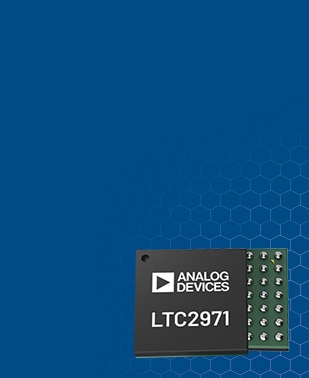
Analog Devices LTC2971 2-Channel Power System Managers | New Product Brief
Analog Devices LTC2971 2-Channel Power System Managers actively manage and supervise two switching converters with outputs from negative 60 volts to positive 60 volts.
Selecting the Best Power Solution for RF Signal Chain Phase Noise Performance
This article investigates the effect that power designs have on the phase noise of RF amplifiers.
What Is Phase Noise?
Phase noise is the noise in a signal that comes from an unexpected lead or lag when the signal arrives at the receive side of a system. Just as amplitude noise is a shift or deviation from the signal’s nominal amplitude, phase noise is a shift or deviation from the signal’s nominal phase.
Cause and Contribution of Phase Noise
A critical and often-overlooked cause of phase noise is the DC power solution of the signal chain. Any noise or ripple on the power rails that supply the signal chain can couple internally. This can lead to an increase in phase noise, which may hide critical frequency components in the bandwidth transmitted or could induce spurs offset from the carrier.
Power Solutions
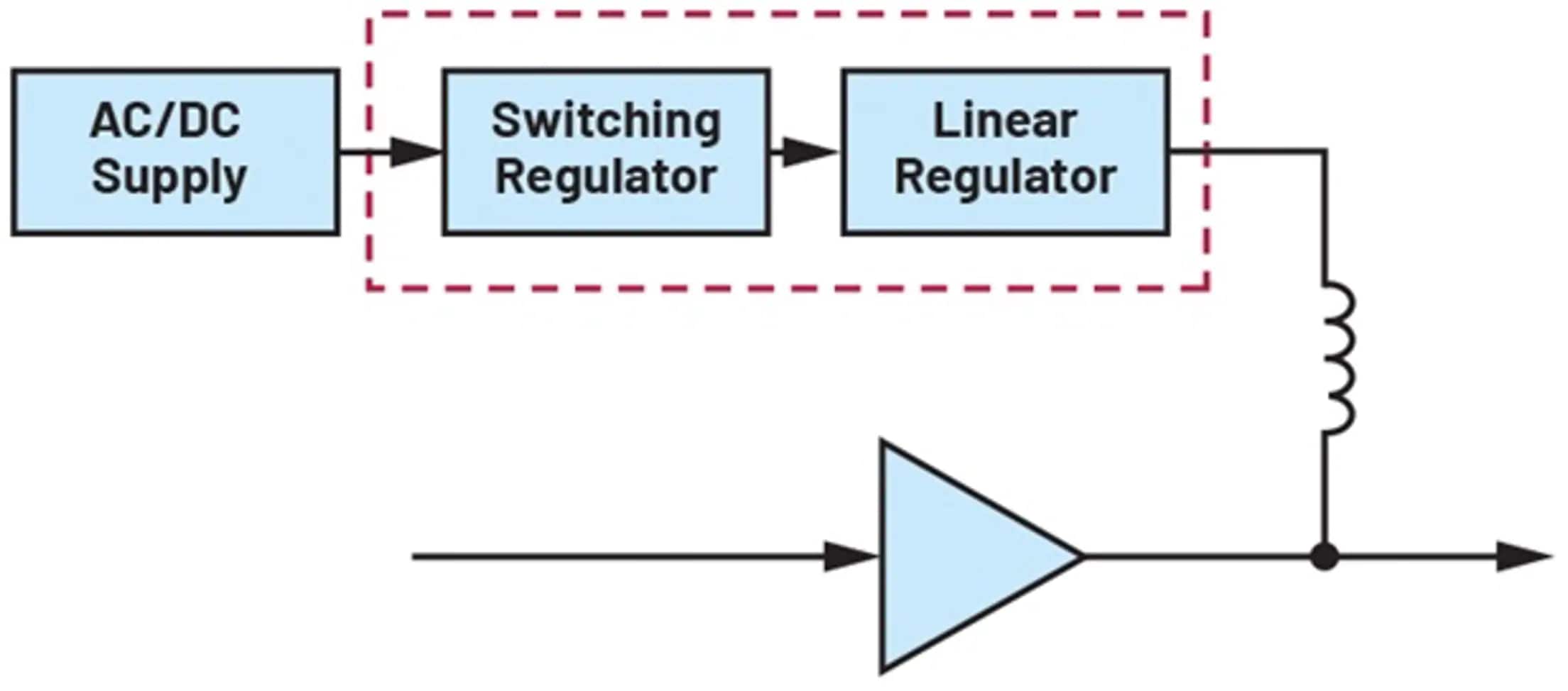
Ensuring proper biasing and power supply to amplifiers in an RF signal chain can be challenging, especially with drain voltages also used as the output port. There are numerous types of power solutions and topologies on the market. Which power solution you may need will depend on your application and system requirements. For this experiment, the data gets obtained using low dropout (LDO) linear regulators and step-down or buck switching regulators (Figure 1).
Setup
Analog Devices experimented by utilizing three different Analog Devices’ power products: LTM8063 40VIN, 2A Silent Switcher µModule Regulator, LTM4626 µModule Regulator, and LT3045 Power Supply Rejection Ratio (PSRR) Linear Regulator (Table 1).
| Table 1. Data Sheet Specifications of Power Solutions Used | |||
|---|---|---|---|
| LTM8063 | LTM4626 | LT3045 | |
| Topology | Buck µModule® | Buck µModule | LDO regulator |
| Input Voltage Range | 3.2V to 40V | 3.1V to 20V | 1.8V to 20V |
| Output Voltage Range | 0.8V to 15V | 0.6V to 5.5V | 0V to 15V |
| Output Current | 2A | 12A | 500mA |
| Noise | ~15mV ripple | ~35mV ripple | 1μV rms |
| Switching Frequency | 200kHz to 2MHz | 600kHz to 2MHz | — |
| Table 2. Data Sheet Specifications of RF Amplifiers Used | ||
|---|---|---|
| HMC8411 | ADPA9002 | |
| Frequency Range | 10MHz to 10GHz | DC to 10GHz |
| VDD (typ.) | 5V | 12V |
| IDD (typ.) | 56mA | 385mA |
| Gain | 15.5dB | 15dB |
| Output P1dB Compression (typ.) | 20dBm | 29dBm |
Results
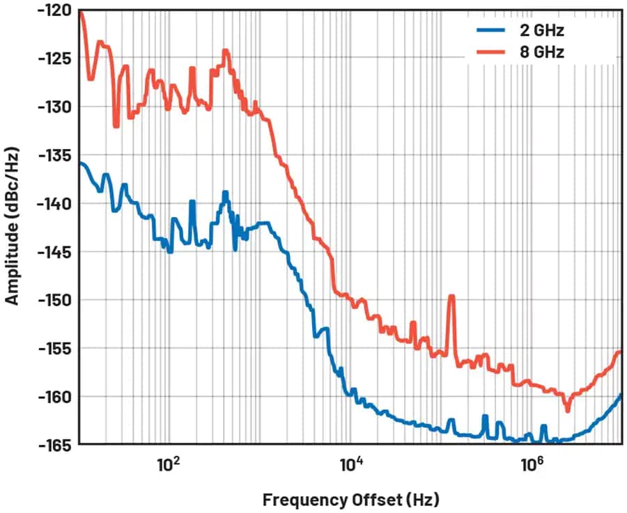
The power amplifier (PA) is observed to have slightly lower performance past 1/f frequencies. The PA draws substantially more supply current, resulting in roughly a 2dB to 4dB increase in observed phase noise (Table 2(a)(b), 3).
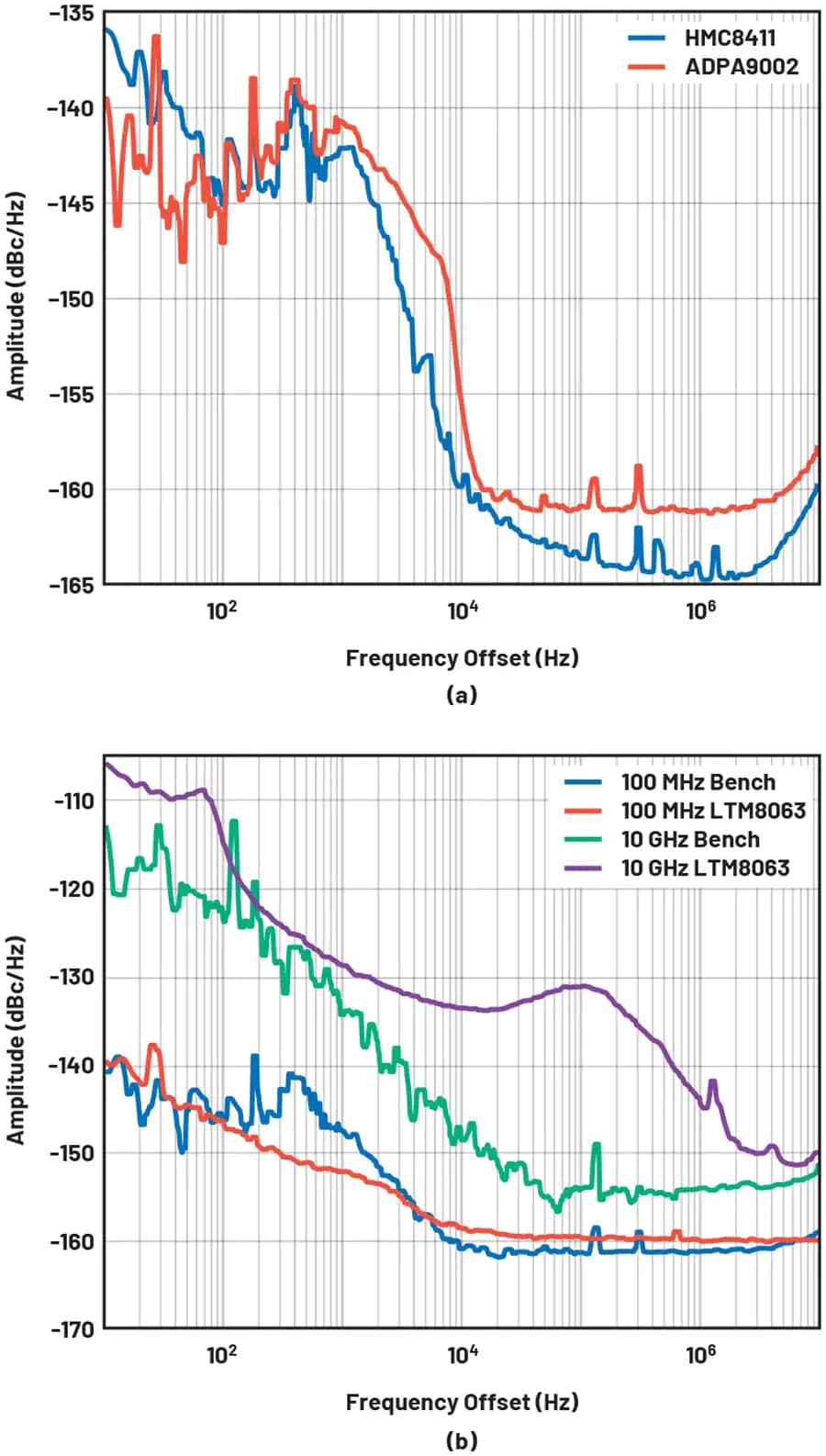
This relationship shows every doubling of the input frequency results in roughly a 6dB increase in phase noise. This can be seen with a 4× increase in frequency, resulting in approximately a 12dB increase from 10Hz to 100Hz frequency offset.
Bench supply phase noise response was used as a baseline to judge the performance of specific power solutions. The LTM8063 has exceptional performance across various frequencies compared to the bench supply, with only an approximate 2dB increase in the wideband noise floor (Figure 4).
Commonly, a high current module such as the LTM4626, will be used as the main supply so that the power distribution network can get stepped down according to each circuit block’s requirements. In this example, the LTM8063 exhibits similar phase noise performance to the LTM4626 cascaded with the LT3045 ultralow noise LDO regulator (Figure 5). If the voltage and current output supplied by the LTM8063 can satisfy design requirements, this power solution can save considerable cost and board space.
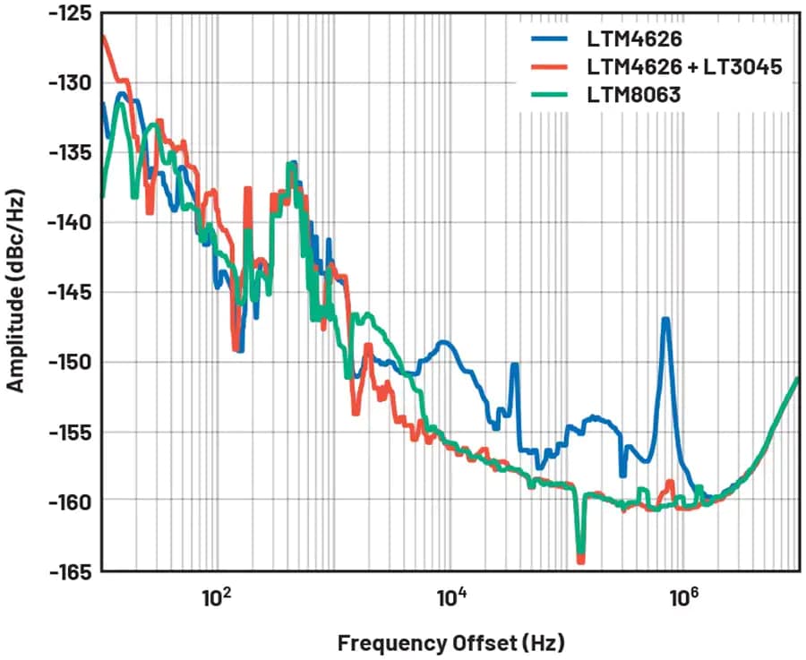
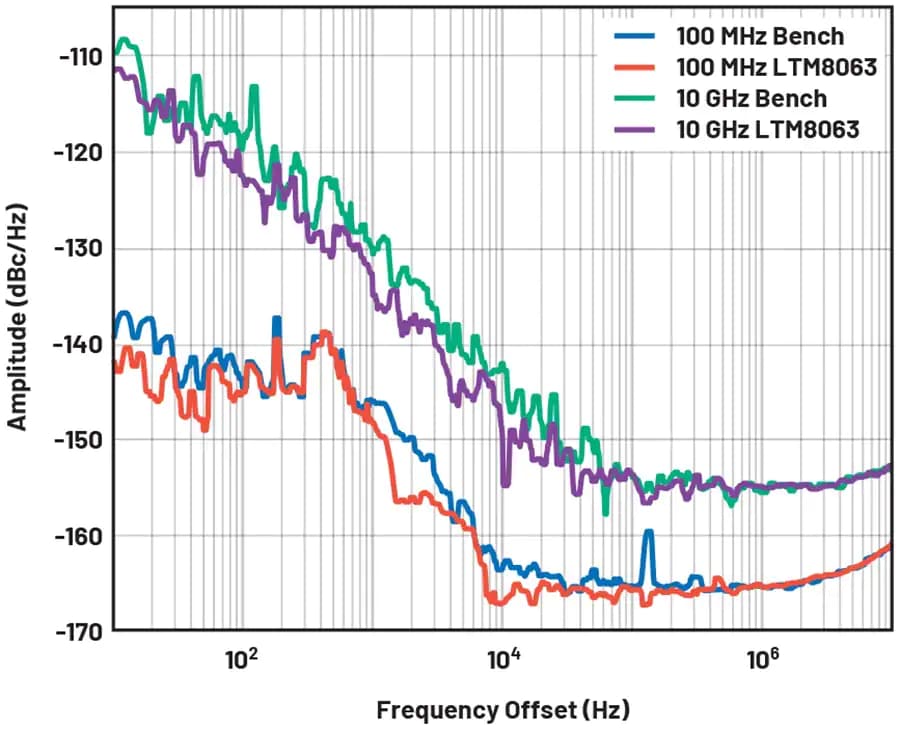
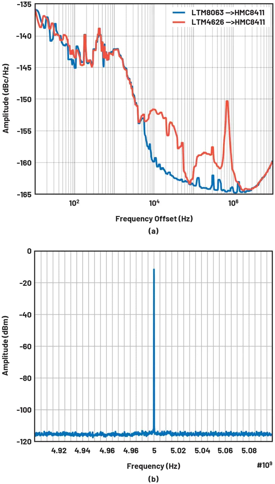
The switching power supplies exhibit markedly different behavior in various frequency bands (Figure 6a). The LTM8063 and LTM4626 have similarly negligible impact on the power low noise amplifier (LNA) phase noise below 5kHz but diverge significantly above that.
The LTM4626 was designed and optimized to power high-end digital products. These devices typically demand high efficiency and fast transient response. Their power supplies may have low passive impedance, fast switching edge rates, and increased control loop gain and bandwidth. These features can create a few millivolts (mV) of perturbations in the output voltage. Though inconsequential in a digital system, these perturbations can degrade the performance of a signal chain product. Despite this, the output spectrum using the LTM4626 showed no noticeable spurs with a spurious-free dynamic range (SFDR) of 102.7dB (Figure 6b).
The LTM8063, however, was designed for low noise—both electromagnetic interference (EMI) and output—optimizing its performance in signal chain applications. It exhibits excellent low-frequency stability, small output perturbations, and much less noise at the switching fundamental and its harmonics.
Conclusion
Considering all noise sources when performing a signal chain analysis is essential. One commonly overlooked source is the DC power solution, which can couple to and severely degrade the performance of the signal chain. Our results show that proper choice of power modules is paramount and can lead to a 10dB improvement of phase noise at 10kHz offset. For this application, the LTM8063 returned the best results. While the LTM4626 cascaded with the LT3045 gave comparable phase noise performance, knowing the correct power solution to choose is critical for optimizing your RF signal chain.
The full article may be viewed at How to Select the Best Power Solution for RF Signal Chain Phase Noise Performance.
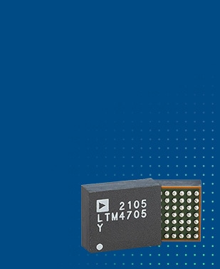
Analog Devices LTM4705 DC-DC μModule® Regulator | New Product Brief
Analog Devices’ LTM4705 is a complete dual 5A step-down switching mode micromodule regulator in a tiny 6.25mm × 7.5mm × 3.22mm BGA package.
Protect and Power Vehicle-Asset Tracking Devices
Introduction
Vehicular asset tracking is an essential part of fleet management, providing a way to know the exact location of physical assets around the clock. The three main benefits of asset tracking are cost savings, theft protection, and preventative maintenance. This article describes how to power the device with a small, efficient power solution and how to protect it from electrical stresses in a vehicle environment adequately.
Vehicular Asset-Tracking Power Requirement
Vehicular asset-tracking/fleet-management devices get powered by the vehicle's battery, typically 12V in cars and 24V in many trucks. As an aftermarket add-on, they face a much harsher power management environment than a well-bounded OEM device. Most devices also have a rechargeable backup battery, typically 3.6V, intended to last two or three days when the main battery power is lost. The primary battery source protects the front-end electronics against transient and fault conditions. The protected voltage gets converted to useable, lower voltages (5V, 3.3V, 2.5V, or 1.2V) by step-down DC-DC converters and LDOs to power various digital logic and analog ICs (Figure 1).
Powering the Device with Modern DC-DC Regulators
Asset-tracking/fleet-management devices must be physically small to fit in small places. In such a small area, reducing the heat dissipation in a device to keep its temperature within range is a challenge. Fitting the power circuit into a small space requires high integration. Modern DC-DC regulator power solutions that effectively integrate the power MOSFETs, compensation circuits, and other external components help reduce overall circuit size. Combining the small solution size with the efficient synchronous rectification technology helps reduce the power dissipation. To increase integration, Himalaya uSLIC™ power modules also integrate the power inductor and other discrete components with the DC-DC regulator. This easy-to-use, easy-to-design, and quick time-to-market power module solutions only require an input capacitor, an output capacitor, and an optional soft-start setting capacitor to complete the power solution. The uSLIC family employs advanced packaging technology to minimize the module footprint. For example, the modules fit a 60V, 300mA power solution into a tiny, 2.6mm x 3mm x 1.5mm power module. This highly efficient synchronous DC-DC buck power module also minimizes the heat dissipation in end equipment. The MAXM15062 has a fixed 3.3V output, while the MAXM15063 is similar but with a fixed 5V output. Analog Devices’ employs these two modules to power our example asset-tracking/fleet-management device.
One might consider employing LDOs here for small size since LDOs are generally low cost and very simple to use, but they have high power dissipation if used directly from the primary battery voltage, which is the main drawback. Dissipating this power in a small asset-tracking device may be impractical and may cause device overheating. A solution that can meet both size and power dissipation requirements is required. The MAXM15062/MAXM1563 uSLIC power module fits the bill here. Total power dissipation employing the uSLIC power modules provides an 18x power dissipation reduction compared to the LDOs solution. Low power dissipation also means lower system operating temperature and higher long-term reliability.
Protecting the Device from Faults
Electronic components can encounter short-circuit faults. Short-circuit and overcurrent protection circuitry is essential for preventing fire hazards and isolating the power cable from a failed-short device.
When the ambient temperature becomes excessive or if there is an overcurrent or some other fault, the overtemperature protection prevents permanent damage by either scaling down the power or shutting down the device completely. Overtemperature protection prevents system overheating and fire hazards. It also ensures that the system operates within its defined temperature limits.
Reverse voltage faults occur when the battery gets connected in reverse, or the power cable is installed backward. While unlikely to happen, reverse voltage faults usually cause expensive damage to the power cables and electronic devices connected to the cable without proper reverse voltage protection.
Analog Devices MAX17608 60V/1A current limiter is a highly integrated IC that packs all necessary protections into a single, tiny 3mm x 3mm, 12-pin TDFN package (Figure 2). Some of the MAX17608 features are:
- High input voltage tolerance (+4.5V to +60V operating range)
- Reverse voltage protection (tolerates -60V negative input voltage)
- Reverse current protection
- Short-circuit overcurrent protection
- Adjustable OVLO, UVLO, startup current, and forward current limit
- Overtemperature protection
Conclusion
Vehicular asset-tracking/fleet-management devices are designed to operate from the vehicle’s 12V/24V battery system and must fit in small places. They must be robust against transient conditions, including overvoltage, overcurrent, reverse voltage, reverse current, and overtemperature. Highly integrated protection ICs provide all the above protections and simplify the design over discrete solutions. Highly integrated and efficient uSLIC power modules ensure fit, mitigate thermal dissipation challenges, and enhance the long-term reliability of the device.
The full article may be viewed at Protect and Power Vehicular Asset-Tracking Devices.
Power Supply Subsystems for Remote Patient Vital Sign Monitoring
Introduction
This introductory article is part of an entire series guiding designers to implement and validate a proven switch-mode power supply (SMPS) circuit for use in remote vital sign monitoring devices using Analog Devices’ biosensing analog front ends (AFEs) (Figure 1).
Switching mode power supplies offer high efficiency and compact footprint optimal for remote patient monitors. However, designs must ensure that each Analog Devices’ biosensing device’s signal-to-noise ratio (SNR) performance is not adversely affected by high-frequency switching noise. High-frequency switching noise can get aliased in-band where vital sign signals get sampled to avoid performance degradation.
Analog Devices offers designers pre-validated power supply circuits for use with biosensing devices. In addition, each power supply circuit example is complemented with a validation checklist and troubleshooting guide to aid circuit designers if needed.
Who Should Read This?
Designers developing remote patient vital sign monitors and consumable diagnostic devices using Analog Device's biosensing AFEs (Table 1).
| Analog Devices Part Number | Function |
|---|---|
| MAX30001CWV+ | ECG, R-to-R, Pace, and BioZ Biosensor |
| MAX30003CWV+ | Ultra-Low Power, Single-Channel Integrated Biopotential (ECG, R to R Detection) AFE |
| MAX30004CWV+ | Ultra-Low Power, Single-Channel Integrated Biopotential HR Detection AFE |
| MAX86140ENP+ MAX86141ENP+ |
Optical Pulse Oximeter and Heart Rate Biosensor (MAX86140 Single Channel; MAX86141 Dual Channel) |
| MAX86176ENX+ | ECG, Optical Pulse Oximeter, and Heart Rate Biosensor |
| MAX86131CWA+ | Electrochemical Biosensor |
| MAX30208CLB+ | ±0.1°C Accurate, I2C Digital Temperature Sensor |
Retrieving actionable information from biosensor data requires excellent system signal-to-noise performance. Adopting Analog Devices’ AFEs is the first step toward this goal. Designers should take the next step: Build a sound power supply design.
Analog Devices pre-validated solutions guide designers to:
- Select a power supply configuration based on system requirements
- Use reference circuits and layouts of both discrete and integrated designs
- Adopt a power supply performance test methodology to validate the system over different device use cases and transient loading conditions
- Utilize a comprehensive checklist to validate their implementation
- View test data expected from a successful implementation
- Apply system integration guidelines
- Follow troubleshooting instructions to address issues
Remote Patient Monitor and Medical Wearable System Configurations
Analog Devices pre-validated solutions apply to designs with the following requirements:
- Small system form factor and low mass
- Maintains good battery life with low battery mass and cost. Most of the systems get kept in standby or low power state
- Very high signal-to-noise performance at sampling rates below 1kHz
- The design employs one or more (primary or secondary) batteries with a nominal voltage ranging from 0.9V to 4.2V. For example:
- LP401230 3.7V 105mAh Secondary (Rechargeable) Cell LiPo Battery
- BR2032 3.0V 190mAh Primary (Non-Rechargeable) Cell Battery
- CR2032 3.0V 235mAh Primary (Non-rechargeable) Cell Li Battery
- Includes devices that require one or more voltage rails, for example:
- 1.8V for digital devices (VDIG) with fast transitions and high operating current
- 1.8V analog supply (VANA) where power supply noise affects sensor data integrity
- 5V supply for LED currents (VLED) in optical systems
Analog Devices’ rechargeable power system configuration gets designed to work with input voltages ranging from 3.0V to 4.2V, typical of Li-Ion or LiPo rechargeable batteries. Three outputs get generated: Two 1.8V supplies (VANA and VDIG) and one 5V supply (VLED). Figure 1 above shows a block diagram where one supply is a tightly regulated 1.8V digital supply to power the digital sections of a microcontroller where noise is typical with fast transitions of digital signals.
Battery Choices for Wearable Applications
Common wearable battery types can be categorized into two (2) basic groups: Primary cell (non-rechargeable) and secondary cell (rechargeable) batteries. Examples of primary cell batteries include alkaline, Li-ion, zinc-air, and silver-oxide varieties, whereas secondary cell battery examples include lithium Ion and lithium polymer (LiPo or LiPoly) cells. Lithium-ion and lithium polymer batteries for wearable applications get favored due to size, mass, rechargeability, energy density, and eco-friendliness.
The designer should know that each battery type will have its own electrical characteristics (e.g., voltage output level, energy storage level, charge/discharge behavior, etc.). Thus, an appropriate switch-mode power supply (SMPS) circuit will need to get implemented for each battery type. In addition, as newer battery types get deployed, the engineer will need to evaluate, characterize, and possibly re-design their power supply circuits accordingly.
Switch-Mode Power Supply (DC-DC Converter) Circuits
Analog Devices’ Switch-Mode Power Supply (DC-DC Converter) Circuits highlight operational details of known good reference designs, including:
- Circuit description, including web links to applicable design files (schematic/BOM/layout)
- Validation checklist to confirm the implemented circuit function
- Selecting test data plots highlighting secondary typical operating characteristics
Both discrete and integrated switch-mode power supply options get offered to help designers accommodate their specific PCB layout requirements.
Two Highlighted Power Components
Analog Devices MAX3864xA/B nanoPower Buck Converters employ a unique control scheme that allows ultra-low quiescent current and high efficiency over a wide output current range (Figure 2). The MAX3864xA/B Converters feature an operating voltage of 1.8V to 5.5V while supporting load currents of up to 175mA, 350mA, and 700mA. Additional benefits of the series include a 330nA ultra-low quiescent supply current, a 5nA shutdown current, and 96% peak efficiency. The Buck Converters are excellent for battery applications where extended battery life gets demanded.
Analog Devices MAX20343/MAX20344 Buck-Boost Regulators offer a 1A current capability at 3.5V intended for applications that require long run times while also demanding bursts of high current (Figure 3). The MAX20343/MAX20344 employs a unique control algorithm that seamlessly transitions between buck, buck-boost, and boost modes, minimizing discontinuities and subharmonics in the output voltage ripple. The MAX20343/MAX20344 features a low 1.9V input voltage for the startup that allows users to power the device from various sources. The MAX20343/MAX20344 design keeps inductance and output capacitance requirements as low as possible for space-constrained applications.
Learn More
The full article may be viewed at Power Supply Subsystems for Remote Patient Vital Sign Monitors. This document offers descriptions of pre-validated power supply circuits for use with biosensing devices for wearable medical and healthcare applications. In addition, each power supply circuit example is complemented with a validation checklist and troubleshooting guide to aid circuit designers if needed.
Extending Battery Life for Hearables and Wearables

Meeting the Battery Life Demands of Tiny Devices
It is not convenient to have to stop and recharge your earbuds when you are on a long hike or working out. It is expected that hearables, wearables, and other tiny, battery-powered electronic devices will perform reliably for prolonged periods of time. From a design standpoint, these user expectations are a tall order to meet. The form factor constraints dictate the need for a small Li+ battery, which must last a long time between charge cycles and be utilized sparingly. Power supplies, in turn, must meet the distinct and diverse voltage requirements of the sub-systems within the design. Single-Inductor Multiple-Output (SIMO) architecture provides an optimal solution for these systems, integrating functionality that would otherwise require multiple discrete components.
SIMO Architecture Overview
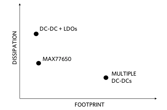
In a traditional switching-regulator topology, each switching regulator needs a separate inductor for each output since each voltage rail must be serviced by an individual inductor (Figure 1). The inductors are physically large and costly, so this is a disadvantage for small form factor products. Linear regulators offer another option—they are fast, compact, and low noise, but they are also lossy. There’s also the hybrid alternative of using multiple low-dropout regulators (LDOs), in conjunction with DC-DC converters. However, while this configuration would result in intermediate power and heat dissipation, it still yields a larger design than LDOs alone.
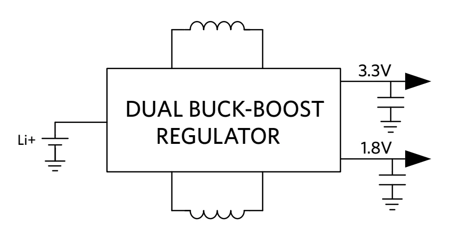
The featured buck-boost SIMO converter can regulate up to three (3) output voltages over wide output voltage ranges using a single inductor. The buck-boost topology helps to better utilize the inductor since it requires less time to service each channel as compared to a buck-only SIMO. The weakness of a buck-only SIMO is magnified as one or more output voltages approach the input voltage. A buck-only SIMO will suffer when an output voltage approaches the battery voltage. Currently, a buck-only SIMO requires the inductor for too much time, which impacts other channels.
Sometimes, an inductor cannot be avoided in the system. Even though they are small, an LDO can never provide a boost feature by itself. Since the SIMO requires only one inductor, solutions that require at least one boost voltage are almost always better with a buck-boost SIMO (Figure 2).
The inductor saturation current (Isat), a measure of the inductance drops to a certain percentage that corresponds to a particular electrical current, is proportional to the inductor’s core size for a given core material and construction. Using one inductor in a SIMO architecture offers various advantages versus using separate DC-DC converters:
- Better Z-height
- Cost savings and footprint improvements
- Time multiplexing
- Lower RMS (current rating for inductors)
Overcoming SIMO Architecture Compromises
Using a SIMO architecture is not without tradeoffs. A thoughtful approach to the design is important. The output voltage ripple will often be higher because there is a single inductor providing buckets of energy to alternate outputs. Also, as a SIMO is heavily loaded, it becomes time-limited and there can be a delay in servicing each channel, which can further increase output voltage ripple. Using larger output caps offsets these sources of output voltage ripple while maintaining a net footprint/BOM advantage.
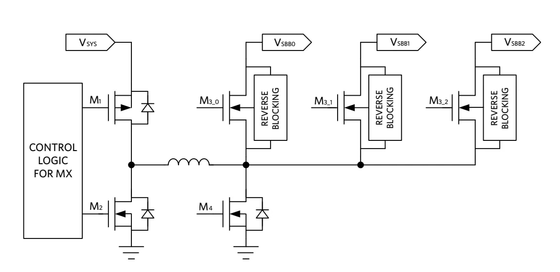
Analog Devices’ MAX77650/MAX77651 Ultra-Low Power Management Integrated Circuits (PMICs) provide a careful balance of these tradeoffs. These PMICs were designed with micropower SIMO buck-boost DC-DC converters. An integrated 150mA low-dropout regulator (LDO) in the PMICs provides ripple rejection for noise-sensitive applications such as audio.
The SIMO converter utilizes the whole battery voltage range, as each output has the benefit of being a buck-boost configuration, which creates output voltages that are above, below, or equal to the input voltage. Since the peak inductor current for each output is programmable, you can optimize the balance between efficiency, output ripple, electromagnetic interference (EMI), PCB design, and load capability.
The SIMO converter utilizes the whole battery voltage range, as each output has the benefit of being a buck-boost configuration, which creates output voltages that are above, below, or equal to the input voltage. Since the peak inductor current for each output is programmable, you can optimize the balance between efficiency, output ripple, electromagnetic interference (EMI), PCB design, and load capability.
This SIMO architecture finds the optimal balance between low power consumption and form factor. The low power consumption can be very important for very small applications that are unable to dissipate much heat (Figure 3).
The SIMO control scheme in the MAX77650/MAX77651 involves a proprietary controller that ensures that all the outputs get serviced in a timely manner. If there aren’t any regulators requiring service, the state machine simply rests in a low-power state. Once the controller recognizes that a regulator needs service, it charges the inductor until the peak current limit is reached. The SIMO architecture also offers a soft-start feature, which minimizes in-rush current.
Summary
For hearables, wearables, and similarly small, battery-operated electronics, long battery life is essential for customer satisfaction. Compared to traditional buck-boost topologies, the SIMO architecture reduces component count and often extends battery life. This paper examined PMICs integrated with SIMO switching regulators that are ideal for meeting the challenges of ultra-low-power, space-constrained applications.
The complete article may be viewed at SIMO Switching Regulators: Extending Battery Life for Hearables and Wearables.
Powering IoT Devices for Long Life
This article presents a specific Internet of Things (IoT) power management solution for small, portable gadgets while also reviewing its shortcomings (Figure 1). We then introduce a nano-Power boost converter that overcomes these shortcomings while ‘operating on fumes’ down to minimal amounts of residual battery energy.

Typical Wearable Power Solution
A wearable heart monitoring patch (Figure 2) is typically tiny and must last a long time; hence, minimization of the size and power dissipation is crucial. This device, powered by a 100mAh alkaline button cell and consuming 100µA in operation, will last three weeks. On the other hand, in shutdown mode, the device may need to last up to three years, which requires a leakage current of 4µA or less. A typical voltage regulator, with a leakage current of 0.2µA and a total quiescent current of 10µA, will rob 1.8 months from the device’s shelf life and two days of operation.

High efficiency and small size are challenging requirements. Increasing the frequency of operation will reduce the size of passives while increasing losses, thereby reducing efficiency. The proliferation of portable IoT devices creates a need for multiple customized versions of voltage regulators, especially concerning the output voltage and current specifications. Accordingly, an IoT device manufacturer may get forced to maintain a sizeable and costly inventory of different regulators and the passives required to support them.
A State-of-the-Art Solution
The ideal solution is a voltage regulator that addresses these shortcomings. Analog Devices MAX17222 nanoPower synchronous boost converter is such a device. The MAX17222 offers a 0.4V to 5.5V input range, a 0.5A peak inductor current limit, and an output voltage selectable using a single standard 1% resistor.
A novel True Shutdown™ mode yields leakage currents in the nanoampere (nA) range, making this a genuinely nanoPower device!
True Shutdown Current Advantage
The essential elements of the MAX17222 concerning shutdown and quiescent currents are shown below (Figure 3).
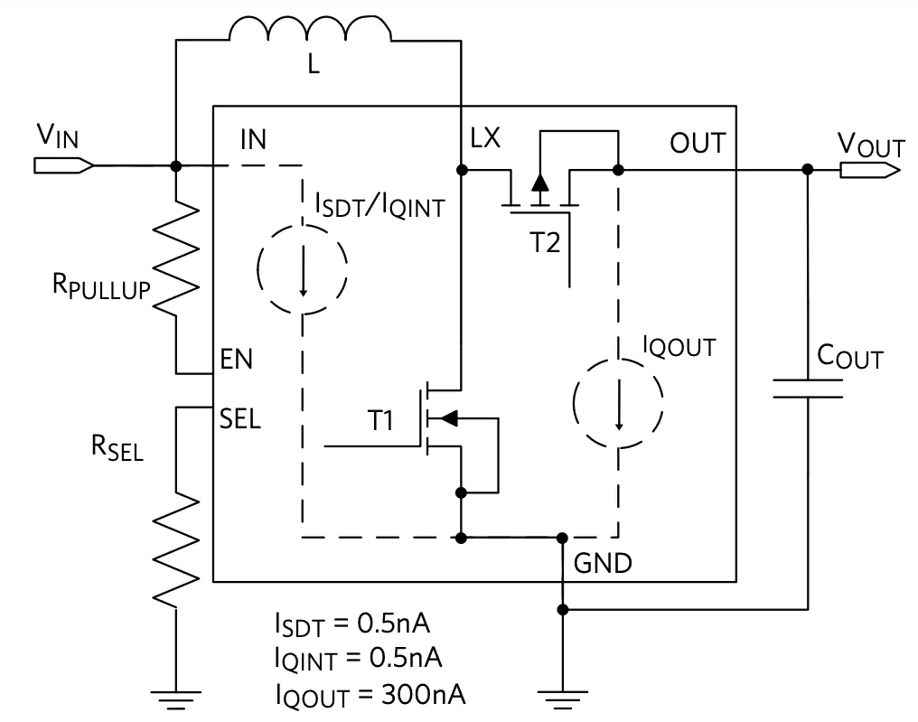
The True Shutdown feature disconnects the output from the input with no forward or reverse current, resulting in a very low leakage current. If you recall, the reduction in shelf life we calculated for the specific solution is 1.8 months out of three years for a 100mAh cell. With 0.5nA leakage current, the shelf life for the same cell over three years gets reduced to only three hours.
If a pull-up resistor is employed to enable/disable operation, the pull-up current in True Shutdown mode must also get accounted for. If the enable (EN) pin gets driven by a push-pull external driver powered by a different supply, then there is no pull-up current, and the shutdown current is only 0.5nA.
Quiescent Current Advantage
The input quiescent current (IQINT) for MAX17222 is 0.5nA (Enable open after startup), and the output quiescent current (IQINT) is 300nA (Figure 3). The additional input current needed to feed the output current (I>QINT_IN) must be added to IQINT to calculate the total input quiescent current. Since the output power is related to the input power by the efficiency (POUT = PIN × η), it follows that:
I>QINT_IN = IQOUT × (VOUT/VIN)/η
If VIN = 1.5V, VOUT = 3V and efficiency η = 85%, we have:
I>QINT_IN = 300nA × (3/1.5)/0.85 = 705.88nA
One adds the 705.88nA to the input current of 0.5nA to yield a total input quiescent current of 706.38nA (IQINGT). This calculation is fourteen times better than the typical case previously discussed. With 0.7µA of quiescent current, the two days of reduced operation calculated for the specific solution becomes only three and a half hours.
Enable Transient Protection Mode
The MAX17222 includes an option to enable transient protection (ETP) mode. When activated by the presence of a pull-up resistor, extra on-chip circuitry powered by the output capacitor assures that EN stays high during short transient disturbances at the input. In this case, the quiescent current calculated above increases by a few tens of nanoamps.
RSEL Advantage
The MAX17222 trades off the traditional resistor-divider used to set the output voltage value with a single output selection resistor (RSEL) (Figure 3). The chip uses up to 200μA to read the RSEL value at startup. This occurs only during the select resistor detection time (typically 600µs), virtually eliminating the contribution of RSEL to the quiescent current. A single standard 1% resistor sets one of the thirty-three different output voltages, separated by 100mV increments between 1.8V and 5V! The result is a slight reduction in the bill of materials (BOM), as we now have one less resistor and a lower quiescent current.
Efficiency Advantage
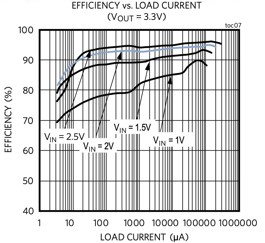
The MAX17222 features low RDSON, on-board powertrain MOSFET transistors to yield excellent efficiency even when operating at frequencies high enough to warrant a small overall PCB size. The low quiescent current design extends the outstanding efficiency performance down to a few microamps of load current (Figure 4).
Conclusion
The IoT market has generated an explosion of small, wirelessly-connected, battery-operated devices. These devices continue to lower the power loss boundaries for operation (efficiency) and shutdown (leakage current). Analog Devices MAX17222 ultra-low quiescent current, high-efficiency synchronous buck converter significantly increases IoT devices’ shelf and operation life. It is an ideal choice for this class of applications.
Photo/imagery credits
deepagopi2011 - stock.adobe.com | Milles Studio - stock.adobe.com