Toshiba TC7PCI321xMT/TC7PCI341xMT Mux/Demux Switches
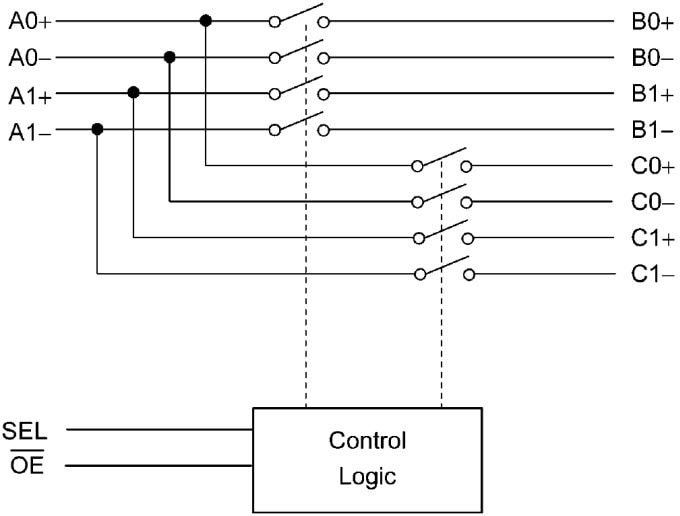
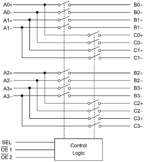
Toshiba TC7PCI321xMT/TC7PCI341xMT 2:1 Multiplexer/Demultiplexer Switches are 2 (TC7PCI321xMT) or 4 (TC7PCI341xMT) differential channel switches for PCI Express Gen3 (8Gbps) or other high-speed interface applications. The An+/An- inputs are connected to the Bn+/Bn- or Cn+/Cn- outputs determined by the combination of both the select input (SEL) and output-enable (OE). When the output-enable (OE) input is held high-level, the Toshiba switches are open (high-impedance state) regardless of the state of select inputs and reducing consumption current. All inputs are equipped with protection circuits against static discharge.Features
- VCC = 3V to 3.6V operating voltage range
- CI/O = 1.5pF Switch On (typ.) @ VCC = 3.3V switch terminal ON-capacitance
- RON = 7.5Ω (typ.) @ VCC = 3.0V, VIS = 0V ON resistance
- -3dB Bandwidth
- TC7PCI3212MT, TC7PCI3215MT BW = 11.5GHz (typ.) @ VCC = 3.3V
- TC7PCI3412MT, TC7PCI3415MT BW = 10GHz (typ.) @ VCC = 3.3V
- DDIL = -1dB (typ.) @ VCC = 3.3V, f = 4GHz insertion loss
- DDOIRR = -20dB (typ.) @ VCC = 3.3V, f = 4GHz Off isolation rating
- DDNEXT = -40dB (typ.) @ VCC = 3.3V, f = 4GHz crosstalk
- ESD Performance
- Machine model ≥ ±200V
- Human body model ≥ ±2000V
- Package
- TC7PCI3212MT, TC7PCI3215MT - TQFN20
- TC7PCI3412MT, TC7PCI3415MT - TQFN42
TC7PCI321xMT Block Diagram

TC7PCI341xMT Block Diagram

Published: 2016-02-16
| Updated: 2022-03-11


