


Texas Instruments SN74LVC244A/SN74LVC244A-Q1 Octal Bus Buffers

Texas Instruments SN74LVC244A/SN74LVC244A-Q1 Octal Bus Buffers contain eight individual high-speed CMOS buffers organized as two 4-bit buffers/line drives with 3-state outputs. Each buffer performs the Boolean logic function xYn = xAn, where x is the bank number and n is the channel number. These octal bus buffers are designed for 1.65V to 3.6V VCC operation and for asynchronous communication between data buses. The Texas Instruments SN74LVC244A-Q1 devices are AEC-Q100 qualified for automotive applications.
Features
- Operates from 1.65V to 3.6V
- Inputs accept voltages to 5.5V
- Specified from –40°C to +85°C and –40°C to +125°C
- Maximum tpd of 5.9ns at 3.3V
- Typical VOLP (output ground bounce) < 0.8V at VCC = 3.3V, TA = 25°C
- Typical VOHV (output VOH undershoot) > 2V at VCC = 3.3V, TA = 25°C
- Supports mixed-mode signal operation on all ports (5V input or output voltage with 3.3V VCC)
- Ioff supports live insertion, partial-power-down mode, and back-drive protection
- Can be used as a down translator to translate inputs from a maximum of 5.5V down to the VCC level
- Available in ultra-small logic QFN package (0.5mm maximum height)
- Latch-up performance exceeds 250mA per JESD 17
Applications
- Servers
- LED displays
- Network switches
- Telecom infrastructure
- Motor drivers
- I/O expanders
- Enable or disable a digital signal
- Controlling an indicator LED
- Translation between communication modules and system controllers
Additional Resources
- SN74LVC244A Datasheet
- SN74LVC244A-Q1 Datasheet
- Selection Guide: Logic Guide
- Application Note: Implications of Slow or Floating CMOS Inputs
- Application Note: How to Select Little Logic
- Application Note: Understanding and Interpreting Standard-Logic Data Sheets
- User Guide: LOGIC Pocket Data Book
- Application Note: Selecting the Right Level Translation Solution
Functional Block Diagram

Development Tools
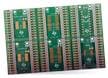
Texas Instruments 14-24-LOGIC-EVM Logic Evaluation Module (EVM)
Generic evaluation module developed to support any TI logic leaded device in a 14 to 24 pin count.
Texas Instruments 14-24-NL-LOGIC-EVM Logic Evaluation Module (EVM)
Supports any logic or translation device in a BQA, BQB, RGY (14-24 pin), RSV, RJW, or RHL package.