


Texas Instruments LMK1D1208I I2C Low-Additive Jitter LVDS Buffers
Texas Instruments LMK1D1208I I2C Low-Additive Jitter LVDS Buffers offer two inputs and eight pairs of differential LVDS clock outputs (OUT0 through OUT7) with minimum skew for clock distribution. The inputs allow a choice of either LVDS, LVPECL, LVCMOS, HCSL, or CML.
The TI LMK1D1208I I2C Low-Additive Jitter LVDS Buffers are intended for driving 50Ω transmission lines. Furthermore, when users are driving inputs in single-ended mode, they should apply the appropriate bias voltage to the unused negative input pin. The device's I2C programming allows configuration as a single bank buffer (one of the two inputs is distributed to eight output pairs) or a dual bank buffer (each input is distributed to four outputs pairs). The LMK1D1208I can configure each output to have either a standard (350mV) or boosted (500mV) swing. The LMK1D1208I combines individual output channel enable/disable through I2C programming. The buffers provide fail-safe inputs that prevent oscillation at the outputs without an input signal and allow for input signals before VDD is supplied.
The LMK1D1208I operates in a 1.8V, 2.5V, or 3.3V supply environment and is distinguished from –40°C to 105°C (ambient temperature).
Features
- High-performance LVDS clock buffer family with 2 inputs and 8 outputs
- Output frequency up to 2GHz
- 1.8V / 2.5V / 3.3V ± 5% Supply voltage
- Device configurability through I2C programming
- Individual input and output enable/disable
- Individual output amplitude select (standard or boosted)
- Bank input multiplexer
- Four programmable I2C addresses through IDX pins
- <60fs RMS maximum in 12kHz to 20MHz at 156.25MHz Low additive jitter
- -164dBc/Hz (typical) Very low phase noise floor
- <575ps maximum Very low propagation delay
- 20ps Maximum output skew
- Universal inputs accept LVDS, LVPECL, LVCMOS, HCSL, and CML
- Fail-safe inputs
- LVDS reference voltage, VAC_REF, are available for capacitively coupled inputs
- –40°C to 105°C Industrial temperature range
- 6mm × 6mm, 40-Pin VQFN (RHA) Packages available
Applications
- Telecommunications and networking
- Medical imaging
- Test and measurement equipment
- Wireless communications
- Pro audio/video
Application Example

Block Diagram

Related Development Tool
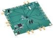
Texas Instruments LMK1D1208IEVM LVDS Buffer Evaluation Module
Demonstrates the electrical performance of the LMK1D1208I, a low-additive jitter LVDS clock buffer.